Chiplet
A small chip designed to be combined with others in one package, like a building block.
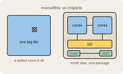
Traditionally a processor is monolithic: one single piece of silicon (a die) holds everything. A chiplet design splits that processor into several smaller dies, each doing one job, such as a group of CPU cores, the input/output and memory controllers, or a cache, and mounts them side by side, or stacked, inside the same package. Very short, very dense connections make them work together almost as if they were one chip.
The main reason is yield. Every silicon wafer has a few random defects; on a huge die, one defect can ruin the whole thing, while on small dies it only ruins one little piece. Smaller dies mean more good chips per wafer and lower cost. Chiplets also let designers mix process nodes: the compute cores go on the newest, most expensive node, and the I/O part, which does not benefit much from it, goes on an older, cheaper one. And one set of building blocks can be reused to make a whole product line, from 8 to 96 cores, just by changing how many chiplets go in.
AMD popularized the approach in its Ryzen and EPYC processors, and today it is common: Intel's recent CPUs, Apple's largest M-series chips (two dies joined together) and the big AI accelerators from NVIDIA and AMD, which place GPU dies next to stacks of HBM memory. The hard part moved from the chip to the advanced packaging that joins the pieces, an area where TSMC is a key player. The UCIe standard aims to let chiplets from different companies plug into each other.
Keep in mind
- Splits one big chip into several small dies inside one package.
- Small dies waste less silicon to defects, so they are cheaper to make.
- Each part can use the process node that suits it best.
- Depends on advanced packaging, now a bottleneck as important as the chips themselves.